
Equipment and Process
Equipment and Processes
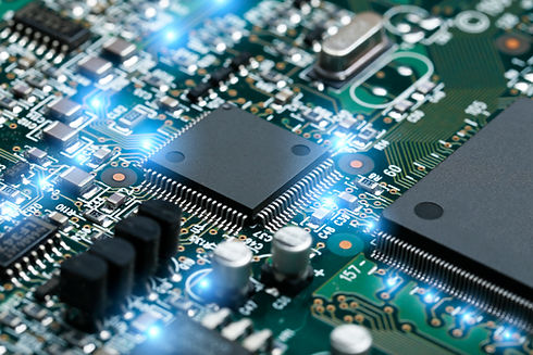
Focus on professional manufacturing of printed circuit boards (PCB).
Create innovative and high-quality products and provide a full range of services from sample prototyping to mass production.

PCB Equipment
PCB Equipment
(1) Exposure: Solder mask exposure machine.
(2) Development: development.
(3) Drilling: Drilling machine.
(4) Copper plating: electroplating of copper and copper.
(5) Printing: Screen printing machine.
(6) Depaneling Machines: PCB Forming Machines
(7) Testing and inspection: professional oven machine.
Manufacturing Time
Manufacturing Time
Exposure
Solder mask exposure machine
Ultraviolet light is used to transfer the design pattern to the photosensitive film covering the copper layer. After exposure, the unexposed parts are removed by development, leaving the desired circuit pattern.


Development
Development
Used to remove unwanted parts from the photosensitive film and reveal the circuit pattern in the PCB design.

Drilling
Drilling Machine
Drill holes on PCB for mounting components or making electrical connections. These holes include through holes and blind vias.


Copper plating
Electroplating copper
A layer of copper is plated inside the drilled hole to connect the copper foil inside and outside the hole to form electrical conduction.


Drilling
Drilling Machine
Drill holes on PCB for mounting components or making electrical connections. These holes include through holes and blind vias.
Screen printing machine.
Print a green solder mask to protect the copper foil from oxidation, and print text or logos on the PCB.


Depaneling
PCB Routing/Depaneling Machine
The process of cutting printed circuit boards (PCBs) into final product sizes, typically carried out during the final stage of PCB fabrication.

Testing and Inspection

Use automated equipment to check the quality of PCBs to detect short circuits, open circuits, defects, etc.

Oven
PCB professional oven machine.

Screen printing machine.
Print a green solder mask to protect the copper foil from oxidation, and print text or logos on the PCB.
%20(1).png)

Screen printing machine.
Print a green solder mask to protect the copper foil from oxidation, and print text or logos on the PCB.
Copper plating
Electroplating copper
A layer of copper is plated inside the drilled hole to connect the copper foil inside and outside the hole to form electrical conduction.
Copper plating
Electroplating copper
A layer of copper is plated inside the drilled hole to connect the copper foil inside and outside the hole to form electrical conduction.

PCB Manufacturing Process
PCB Manufacturing Process
Design and R&D services
Provide professional PCB design and development services, including circuit design, prototyping, design for manufacturability (DFM), etc.
Technical Support
Provide professional technical support and answers to problems encountered by customers during the design and manufacturing process.
Testing and Control
Provide functional testing, environmental testing, aging testing, etc. to ensure that the quality of each PCB meets international standards.
Manufacturing and delivery
Accurate and efficient production processes ensure fast delivery and provide flexible batch production options.
After-sales service
Provide comprehensive after-sales support, including product maintenance, upgrade services and technical consulting.

Manufacturing Time
Manufacturing Time
(1)PCB sample urgent lead time
1-2Days
2~3Days
4~5Days
Start PCB production
Double layer board
Four-layer board, six-layer board
(2)PCB mass production days
5~6Days
7~10Days
10~14Days
Single-layer board
Double layer board
Four-layer board, six-layer board